Core processes & advanced manufacturing for high-reliability PCBs.
2–10oz copper foils, high current & thermal dissipation.
Rogers, Wangling. Low Df/stable Dk for RF, 5G, automotive radar.
Connect inner layers without through-holes, saving space and improving signal density for HDI.
Epoxy filled & planarized vias under pads, ideal for fine-pitch BGAs.
Lasers for microvias down to 0.075mm, high speed, minimal burr.
±0.1mm depth tolerance for blind holes, recesses, heat dissipation grooves.
Removes via stubs in high-speed designs, reduces signal reflection & insertion loss.
Conical/cylindrical recesses for flush screw mounting, secure mechanical fixation.
Tight tolerance (±0.05mm) for solderless press-fit pins.
Metal deposition on board edges for enhanced strength, edge connectors, and EMI shielding.
Gold alloyed with cobalt/nickel, excellent wear resistance. Thickness 0.05–1.27µm.
Applies hard gold only to critical areas (connectors, gold fingers).
Electroless Ni – Pd – Au. Universal for soldering & wire bonding, RoHS compliant, long shelf life.
30–50µ” hard gold on edge contacts for memory modules, PCIe cards, high-cycle insertion.
Temporary protective coating for selective areas; residue-free removal after soldering.
Conductive carbon paste printed for contact points / jumpers. Cost-effective low-current applications.
Half-hole metallized edges for modular PCB soldering directly to motherboards.
Precision V-grooving for panel singulation, clean edges without mechanical stress.
TDR verification, tolerance ±10% (standard). Prevents reflection & crosstalk.
Ultra Small PCBs, Minimum size 2mm × 2mm, 3/3 mil lines, microvias.
Fully compliant with IPC standards — Class 2 for commercial, Class 3 for high-reliability & safety.
| Parameter | Capability |
|---|---|
| Min Line/Space | 3/3mil (2.5/2.5mil for HDI) |
| Min Hole | 0.15mm (mech), 0.075mm (laser) |
| Max. Board Width | 600mm |
| Max. Board Length | 1200mm |
| FR-4 Material | TG140/TG150/TG170/TG180;IT-180A, Ventec VT-901, VT-47, Megtron 6, TUC TU-933+,Halogen-free Material. |
| High Frequency Material | RO4350B/RO4003C/RT5880/RO6002. |
| Hybrid PCB | FR-4+Rogers / FR-4+Rigid polyimide material |
| Hole Wall Copper Thickness | 20μm - 35μm |
| Min. Annular Ring - Vias | 2mil |
| Min. Annular Ring - PTH | 4mil |
| Soldermask Color | Green/White/Black/Yellow/Red/Blue/Purple/Matte Green/Matte Black. |
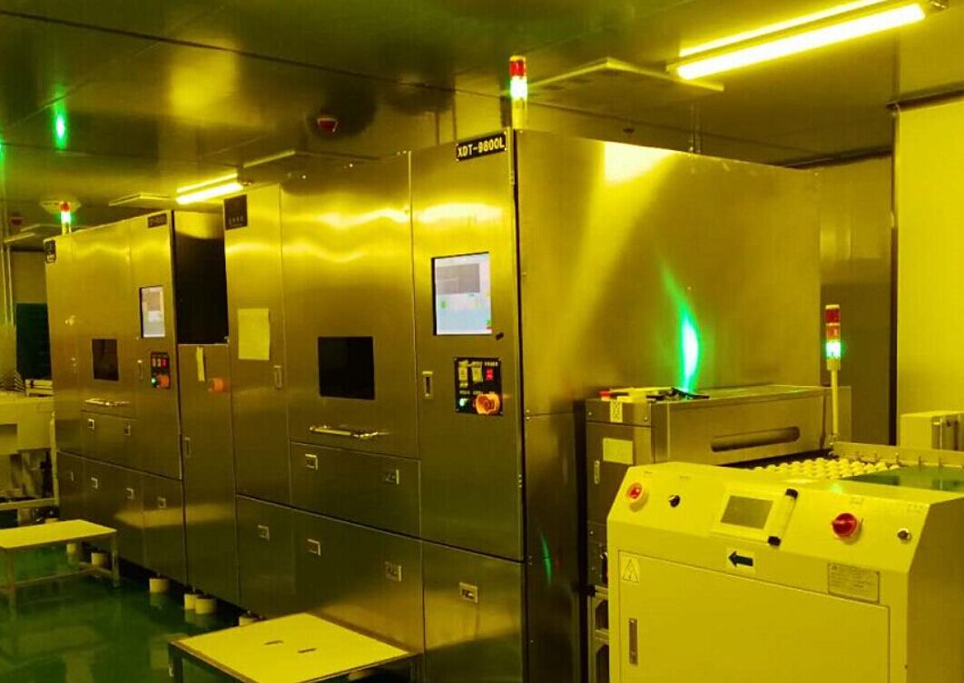
LDI
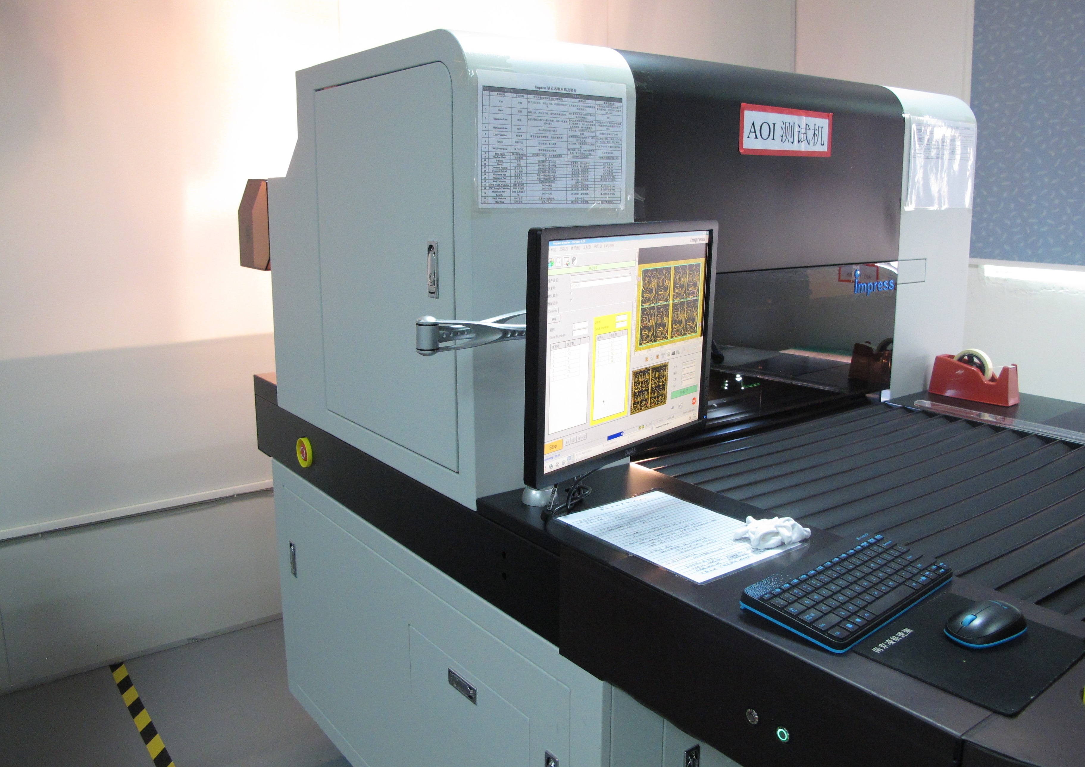
AOI